User Tools

Site Tools


basic_probe_tests

This is an old revision of the document!


Third sample set: Begun 6 May, 2016

This is going to be the same test as I was going to run on sample 2. Because the design did not come out properly after the Heidelberg I am just going to rerun the fabrication process from that step. The design is therefore the same and I hope that this time the design will come out as planned.
The matlab parameters were:
Sample Deminsions:
x=15000um,
y=10000um

Label and Alignment Parameters:
border = 500
textHeight = 500
markSize = 400
lineThick = 30

Probe Waveguide Parameters:
length = 15000
number of probes = 5

Probe 1 width = 1000
Probe 2 width = 3.333333e+02
Probe 3 width = 1.111111e+02
Probe 4 width = 3.703704e+01
Probe 5 width = 1.234568e+01

Second sample set: Begin 5 May, 2016

I am creating a new sample because we found that the waveguides from the previous sample were a little too small. We looked around for them but were not able to find them so they could guide light. This time, we are going to use waveguides that are a little bit bigger so that we can find them easier. We also may postpone the final aluminum etching step until we have found the waveguides and measured their respective angles so we can find them again once we are done.
The matlab parameters were:
Sample Deminsions:
x=15000um,
y=10000um

Label and Alignment Parameters:
border = 500
textHeight = 500
markSize = 400
lineThick = 30

Probe Waveguide Parameters:
length = 15000
number of probes = 5

Probe 1 width = 1000
Probe 2 width = 3.333333e+02
Probe 3 width = 1.111111e+02
Probe 4 width = 3.703704e+01
Probe 5 width = 1.234568e+01
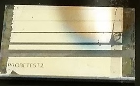
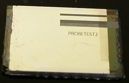
As I performed the aluminum etching, I found a slight problem with my sample. Somehow the settings on the Heidelberg must have been incorrect or different because my sample came out incorrectly. The design printed correctly, it just printed it in the wrong place. Because the design was off center, most of the design is missing and a large portion of the sample was left blank.
I assume that the next thing I should do is probably print the design again on a different sample and start again. I will probably just use Al etch to clear away the aluminum and then put it through the E-beam with the next batch so that I can use it again in the future.

First sample set: Begin 3 May, 2016

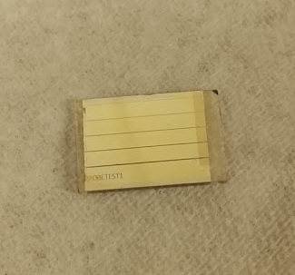
Using a matlab script named basic_Probe I created a test probe. This probe contained a few different rectangles of varying sizes so that we can see how the light reacts to different sized channels.
We took it through the normal process of prepping with S1805::EBR::1:1. Then we sent it through the heidelberg and through the polishing process.

The matlab parameters were
Sample Dimensions:
x=15000um,
y=10000um

Label and Alignment Parameters:
border = 500
textHeight = 500
markSize = 400
lineThick = 30

Probe Waveguide Parameters:
length = 15000
number of probes = 5

Probe 1 width = 120
Probe 2 width = 80
Probe 3 width = 5.333333e+01
Probe 4 width = 3.555556e+01
Probe 5 width = 2.370370e+01

basic_probe_tests.1462567394.txt.gz · Last modified: 2016/05/06 14:43 by rdmclean